

October 10, 2011
AIST Develops New Production Technology for Polycrystalline Silicon Solar Cells
Keywords: Energy Conservation Environmental Technology University / Research institute
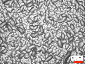
Texture formed in the new process
Courtesy of AIST
The National Institute of Advanced Industrial Science and Technology (AIST) in Japan announced on July 4, 2011, that they have succeeded in developing a new process for manufacturing polycrystalline silicon solar cells, in collaboration with Noritake Co., Fuji Manufacturing Co., and Wako Pure Chemical Industries Ltd.
Whereas polycrystalline silicon ingots are conventionally sliced into wafers using a sawing-wire in an abrasive slurry, in order to reduce cost and environmental load, a new method has been developed using a wire, to which diamond abrasives are fixed, and a coolant. With this method, however, the wafer surface becomes mirror-smooth and low reflectivity cannot be obtained. Therefore, further innovations in the process have been sought to form the desirable texture on its surface at low cost and that are suitable for industrial-scale production.
With further innovations, the wafer is sandblasted to result in the desired asperity on its surface. Then, the wafer is immersed in a newly developed acid-etching solution to remove the blast-damaged layers and create a uniform texture.
The polycrystalline silicon solar cells experimentally made using the new wafers have exhibited good performance characteristics. AIST further aims to verify whether they can be mass produced by improving the sandblasting and acid-etching techniques. Their final goal is to manufacture low-cost, highly efficient polycrystalline silicon solar cells.
Posted: 2011/10/10 06:00:15 AM
Reference
The National Institute of Advanced Industrial Science and Technology (AIST) official website
http://www.aist.go.jp/index_en.html
Related
"JFS Newsletter"
Related
"Popular Articles"
- New Nano-Bubble Technology May Help Dissolve Sludge and Improve Water Quality
- Japanese Firm Begins Development of Tidal Power Generation System
- Small Hydropower Generation System Developed for Use in Seawater, Weight Cut by Half
- Constructed Wetland Facility Established by Japanese University Purifies Livestock Farming Drainage
- Toyota CRDL Succeeds in World's First Artificial Photosynthesis Using only Water and CO2
Related
"JFS' Columns"
![]()

Some rights reserved. This work is licensed under a Creative Commons Attribution-NonCommercial-ShareAlike 3.0 License.